


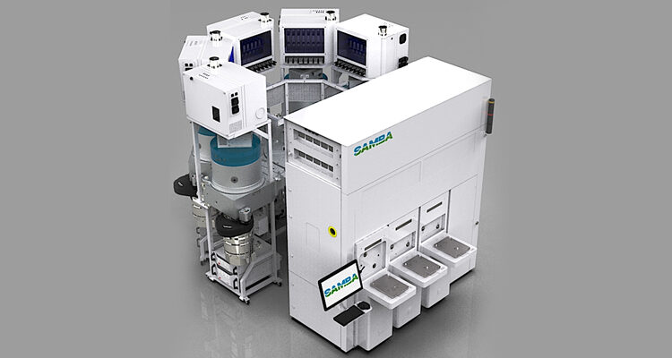
- Plasma dicing
- Through Silicon Via (TSV)
- Via Reveal
- Deep silicon or dielectric etches
Proven Best-in-Class Performance:
Demonstrated leadership across critical process metrics for plasma dicing
Breakthrough Source & Chamber Design:
Precision and uniformity optimized for complex structures
Lower Cost of Ownership:
Optimized consumables strategy for sustained cost efficiency
Compact, High-Throughput Platform:
Maximizes output while minimizing fab footprint
Flexible Architecture:
Seamlessly supports silicon wafers (200/300mm), panel-level packaging, film frame, and glass substrates
Application Flexibility:
Plasma dicing, stress relief, via reveal, TSV/TGV
Valentis is engineered to deliver 2–3× productivity and 2× cost advantage redefining performance benchmarks for advanced packaging
Valentis (Etch): Maintenance friendly and Space efficiency

Access to reach all sub systems on top of EFEM and Process chamber from TC Mezzanine Level
Optimized for high productivity with smaller footprint and improved maintenance efficiency
Valentis (Etch): Cost of Ownership Advantage to Customers
Valentis Etch delivers more than 2X Cost-of-Ownership advantage over conventional Helicon/TCP systems.
Our novel design provides:
- 2–3X higher throughput density – maximize output per square meter
- 60–70% smaller footprint for 10K WSPM capacity – free up valuable fab space
- Low-voltage (<30V) process for reduced consumable costs, improved reliability, and higher yield
Valentis Etch delivers >2X cost-of-ownership advantage, unmatched plasma dicing throughput density, 70% smaller footprint, and significantly lower operating costs