


- EMI shielding (high and low frq.)
- Thick Copper, SuS, Ti, Ni (magnetic materials)
- Dielectrics and Metals
- Barrier/seed layer formation
High Throughput, Low Cost:
3-target co-sputtering enables fewer steps and faster processing
Modular & Scalable:
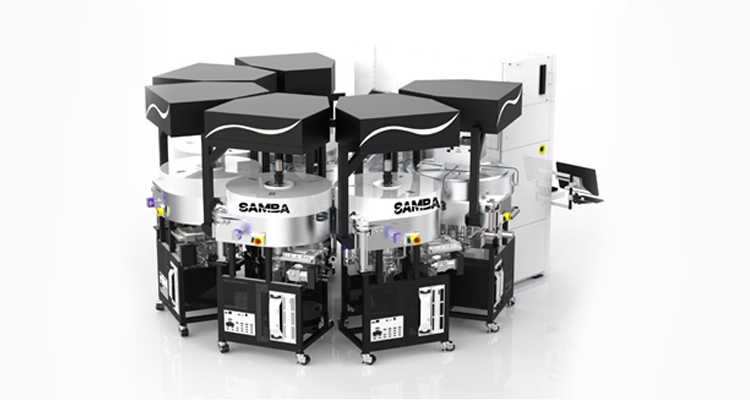
Octagonal architecture w/ flexible chamber and load port configurations
Low Temp, High Performance:
<80°C processing with superior films for advanced packaging
Automation-Ready :
Seamless integration with OHT and factory automation for manufacturing
Flexible & Future Proof:
Supports CVD integration and adapts to evolving substrate needs
Delivering high throughput, low cost, and exceptional process performance
Key Applications
- §Thick Copper, SuS, Ti, Ni (magnetic materials)
- §Barrier/seed layer formation
- §EMI shielding
- §High-rate, low-temp
Best in class performance
- §Low contact resistance
- §Best step coverage
- §High Throughput >75wph
- §Larger targets with high ionization for best CoO
- §Target utilization > 40% (TGV)
- §Pre-clean uniformity <±3%
- §Optimized footprint à 1/4th competitor footprint
- §Spacing between package <1mm

Goal is to deliver 2-3X productivity, 2X cost of ownership advantage to customers