


- Dielectric Gapfill for various applications
- Dielectric films for hybrid bonding
Gaps in Existing Equipment Roadmap to Enable Thick TEOS >>50mm
- Lack of thick oxide solutions is delaying adoption of advanced packaging and chiplet integration
- Customers are forced to overuse thin film tools for thick processes—at high cost & low yield
- Incumbents optimized for thin layers
- High CoO and low throughput for thick oxide
- Limited stress tunability and oxide quality at scale
Segment is underserved – few competitors, rising customer urgency
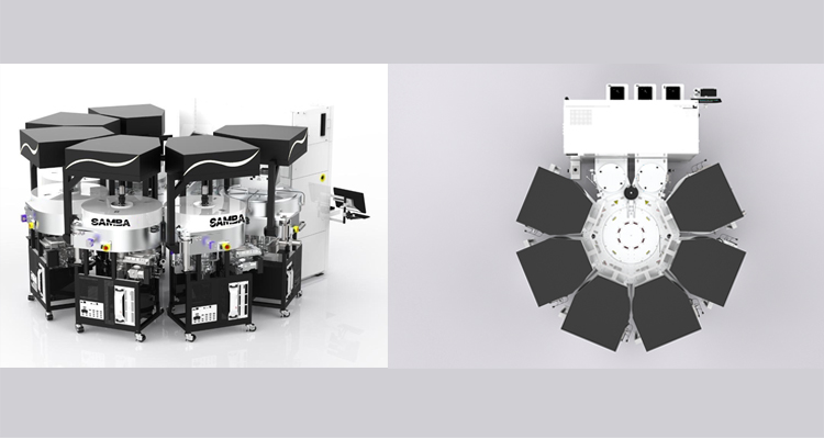
Aquila PECVD: Chamber Designed for Best-in-class Performance at Lower CoO
Key Requirements for thick oxide ≥ 50um
- High Deposition rate (COO)
- Low Stress and tunability (prevent wafer bowing / cracking)
- Uniformity (wafer or panel level)
- Good film quality (density, step coverage, adhesion)
Chamber Design Considerations for Thick TEOS
- High Volume Precursor delivery
- Stable chuck
- Med to High RF
- Bias RF (option)
- Plasma Control (continuous and pulsed)
- Uniformity Control
- Optimized chamber volume
- Moisture Removal (degas – option)
- Integrated metrology (option)
- Small footprint
- Modular and Flexible configuration
Aquila PECVD Differentiation
- High Throughput > 20 wph (normalized for 10-30mm film thickness)
- Tunable film stress for integration flexibility
- Low CoO design — fewer consumables, fewer moving parts
- Compact footprint
- Modular design supports TEOS and SiH4 precursors now for SiO2, SiN, SiON films; future precursors later
- Integrated metrology options for thickness measurement
- Advanced analytics / AI/ML for predictive maintenance, run-to-run control

Purpose built for Thick Oxide Deposition ; Deliver 2X productivity and 2X Cost of ownership advantage
Aquila PECVD – Competitive Positioning : Thick TEOS WLP

Unlocking value in underserved THICK oxide Deposition Market